Two popular low-speed serial buses continue to live on, but changes are afoot in the test and debug equipment used by embedded systems engineers. Philips developed the serial Inter-IC bus (I2C) in the 1980s, and Motorola years ago developed the Serial Peripheral Interface (SPI) bus as an equally simple serial data link between processors and slave devices. I2C uses two wires; SPI uses four (Figures 1 and 2). I2C leaves a smaller footprint and can connect multiple masters to multiple slaves using two wires, but has lower speed performance. On the other hand, SPI offers much faster data rates, but individual lines are required for multiple slaves. Both protocols are simple, work well and are ubiquitous in all kinds of embedded systems—from processors and peripherals to non-volatile memories like EEPROM and Flash to sensors and slow I/O devices.
But ubiquity has its downside. There’s a common belief that debugging systems with these standards is equally simple and straightforward. Not always true. And since they’re so common, designers may think that low-cost rudimentary test and measurement (T&M) tools are “good enough” for these modest buses.
The truth is, evolution of both SPI and I2C demands better tools to debug newer features; remote- and network- equipped T&M equipment is needed in modern engineering and production environments; and “if this, then that” automated style data/event management on both I2C and SPI buses demands more sophisticated equipment to isolate data/events and to debug these complex embedded multi-slave systems. And despite the prevalence of high- speed serial I/O like PCI Express on the latest CPUs and peripherals, SPI and I2C are still appearing on new SoCs, MCUs and peripherals.
To keep up with change, it’s about time for a better T&M tool.
Speed Demons?
In a digital environment, no one is ever going to consider 1 kHz “fast.” Yet the bottom end of I2C clocks at a mere 1 kHz, while SPI starts out at 31 kHz. These low speeds constrain both the Master sending signals on the bus and the speed at which the Slave responds and/or remits data. The faster the clock, the more information can be transmitted per cycle. Test equipment designed to work with SPI or I2C should meet the latest specs—or come close. Trying to debug a system whose speed exceeds the T&M equipment is problematic.
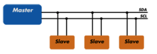
Figure 1: I2C uses a two-wire interface where the lines are shared by the master and multiple slaves and typically maxes out at 1 MHz.
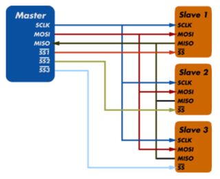 Figure 2: SPI uses a four-wire interface that requires a separate line for each slave and typically clocks up to 8MHz.
An example of the current state-of-the-art is the Aardvark I2C/SPI Host Adapter that supports an I2C Master and Slave at 800 kHz, or an SPI Master at 8 MHz and an SPI Slave at 4 MHz (Figure 3). TotalPhase also offers the Cheetah SPI Host Adapter, a master-only device capable of programming speeds up to 50 MHz.
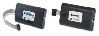 Figure 3: Low-cost USB-connected Aardvark I2C/SPI and Cheetah SPI host adapter T&M equipment.
Evolutionary Improvements to SPI
Since its introduction over 30 years ago, SPI has been used at progressively higher clock rates and lower voltages. Today’s state-of-the-art memory devices operate at speeds up to 133 MHz and operate at voltages as low as 0.9 Volt. In addition to the evolution of voltage and clock rate for standard SPI, Intel is driving the Enhanced Serial Peripheral Interface bus or eSPI as a replacement for the company’s Low Pin Count (LPC) bus. eSPI saves pins compared to LPC (always a plus on an IC) and will operate at up to 66MHz but at a reduced voltage of 1.8VDC. eSPI also differs from SPI by the definition of an Alert# signal that is used by an eSPI slave to request service from the master.
Like SPI, eSPI can be used as a peripheral bus to communicate with sensors in the growing Internet of Tings (IoT) movement. SPI and its variants offer a much faster way to communicate with non-volatile memory such as EEPROM or the more common Flash memory. Popular T&M equipment on the market does not currently support eSPI, so engineers will need to upgrade their hardware when eSPI gains traction. “Upgrade” means set aside the old and buy new.
According to Wikipedia, I2C, which has been popular and stable since its introduction in 1982, has also seen an evolution since its inception :
- In 1982, the original 100 kHz I2C system was created as a simple internal bus system for building control electronics with various Philips chips.
- In 1992, Version 1 added 400 kHz Fast-mode (Fm) and a 10-bit addressing mode to increase capacity to 1008 nodes. is was the rst standardized version.
- In 1998, Version 2 added 3.4 MHz High-speed mode (Hs) with power-saving requirements for electric voltage and current.
- In 2007, Version 3 added 1 MHz Fast-mode plus (Fm+), and a device ID mechanism.
- In 2012, Version 4 added 5 MHz Ultra Fast-mode (UFm) for new USDA and USCL lines, using push-pull logic without pull-up resistors and added assigned manufacturer ID table.
Although now a part of the I2C specification maintained by NXP (which bought the original Philips I2C product line), not all I2C host adapters and T&M equipment support FM+, UFm, or Hs and may be limited to slower (called “standard”) I2C speeds.
One other important point about I2C speeds: the simple two-wire interface and Data/Ack protocol lends itself well to faster speeds. It’s not uncommon for proprietary I2C versions to have faster speeds, limited only by the signal integrity of the wires and connections. T&M equipment that can scale up and accommodate these non-standard faster speeds is highly desirable and becomes obsolete much more slowly, if ever.
Flash Programming
Besides watching the SPI or I2C bus for debug purposes, SPI has become the de facto interface for programming non- volatile memories. SPI-enabled Flash is available from most manufacturers such as Micron and Spansion, and is also used at the Flash module level or on-chip microcontroller interface for easy programming. SPI T&M equipment is the most popular and economical way to program these memories, even in a production (manufacturing) application. But imagine using single-user bench tester equipment in a manufacturing operation.
The downside of using most low-cost SPI programmers for production programming is their need for a host PC and a slow USB 1.1 connection. The USB speed can be alleviated with an upgraded USB 2.0 (480 Mbps) connection, but every SPI T&M box requires an instance of programming software running on its own PC. Although multiple instances can run on a single PC, it’s still a lot of PCs to control locally (and manually) on the manufacturing foor. Even if networked, each PC must be running a virtual machine remotely controlled by the manufacturing engineer via the LAN. Additionally, long distance runs of USB may suffer signal degradation issues, often complicating the production environment by requiring control PCs in close proximity to programming stations.
There’s another downside of using a “simple” SPI programmer in this scenario: each T&M box requires its own USB drivers. Brand “A” will have its own software running on the PC, which will certainly be different from Brand “B.” Maintaining these programmers—and the occasional firmware updates needed to program new memory types and densities—can lead to a challenging configuration management problem. Plus, there’s the PC disk images needed to assure compatibility. These are not insurmountable problems, since this is a common set-up in many manufacturing situations, but it’s a system that is ripe for a better way.
Is Your T&M Equipment on the Level?
As previously mentioned, SPI and I2C are mature technologies that have found their way into countless Master and Slave devices. Their simplicity has made them popular, but the lack of rigorous standards and interoperability certification has left device manufacturers plenty of leeway to create their own protocol variations and voltage levels. This latter issue—voltage—is partially a function of design flexibility and partly due to the digital evolution from 5VDC TTL down to 3.3VDC and lower. For example, Intel’s proposed eSPI goes down to 1.8VDC; some devices accept voltages as low as 0.9VDC.
The trouble is that not all SPI or I2C T&M equipment handles masters or slaves of all voltages. If the target (slave) device operates at 3.3VDC I/O, but the T&M host adapter works at 5VDC, it’s up to the test engineer to create a level- shifter board that converts signals to the appropriate levels. While straightforward, level shifting adds complexity to what should be a simple debug and test environment. Level shifting circuitry adds additional timing delays, can degrade signal integrity and can possibly introduce data or I/O errors due to termination impedance, phase changes and other injected unknowns. It would be ideal if the T&M equipment supported multiple voltage levels, or even programmable ones that match tomorrow’s slave devices.
Future-Proof Features
As we’ve seen so far, despite the simple nature of both SPI and I2C and their decades-long history, both buses continue to evolve (speed, voltage, protocols, proprietary features, etc.). T&M equipment needs to remain flexible enough to “fit” all sizes lest engineers be forced to use multiple host adapters depending upon the device-under-test (DUT). And it’s likely both I2C and SPI will continue to evolve as component vendors consider new protocols and bus commands.
And then there are devices that require interrupts, a feature not covered at all by SPI’s Master-controlled Slave-Select (SS) line. In regular SPI, the Master exerts all the control and only communicates with a Slave when it so desires. But SPI offers an elegant, protocol-agnostic mechanism for streaming d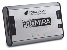 ata from sensors, audio devices, A/D converters and myriad other proprietary I/O.
It would be particularly handy to allow the Slave to interrupt the Master or otherwise offer some feedback ( flow control) mechanism via interrupt. T&M equipment designed for “standard” SPI would have no way of accommodating any kind of custom SPI protocol or extra interrupt line. Yet the common headphone jack on many smartphones is one example of how an interrupt line is used to stop the audio CODEC when the headphones are removed from the jack. What kind of T&M SPI host adapter can test and debug this behavior?
FPGA-based Flexibility
So far we’ve seen that while most I2C and SPI host adapter T&M tools can get the basics done—debugging and programming sensors, MCUs and non-volatile memories— there is room for improvement. In most scenarios, whether a single-user bench set-up, a LAN-based manufacturing line, or faster or non-standard versions of the serial buses, there’s room for additional features in many T&M tools.
TotalPhase, already a leading supplier of I2C, SPI, USB and CAN development tools, is changing the T&M paradigm by creating an FPGA-based, extremely programmable I2C/ SPI solution. Called the “Promira (Latin for “forward” and “miraculous”) Serial Platform,” the device addresses all the challenges and current device deficiencies described above.
To improve speeds between the host adapter and the PC host, both USB 2.0 and 10/100/1000 Ethernet are present. As mentioned above, USB’s 480 Mbps (and double-sized 512 B data packet) reduce timing delays and substantially improve packet transfer between the T&M tool and the PC, allowing faster debugging and data downloads to/from the Promira platform’s greater-than-1 Gbit onboard storage. But it’s the Ethernet LAN connection that really gets noticed. Beyond the faster connection speed—which allows faster non- volatile memory programming—there’s no need for a local PC host for configuration or bottlenecking the throughput.
This makes the device ideal in performance, speed and convenience for factory floor memory programming applications. An optional DIN rail mounting kit allows installation of multiple programmers into industrial racks instead of literally using Velcro to a x programmers to shop fixtures. SPI programming speed has been increased to 80 MHz SPI, dual and quad I/O, and eSPI).
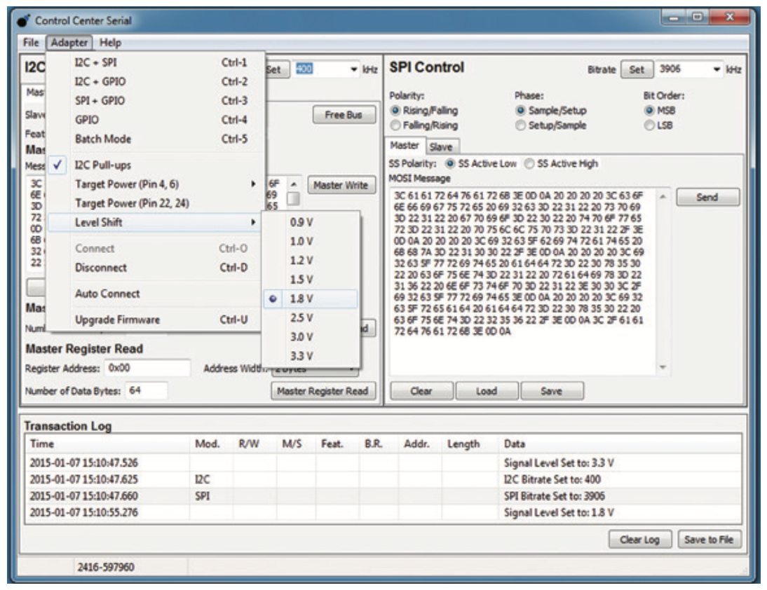
Figure 5: User-programmable level shifting is done via drop- down menu.
LAN connectivity also eliminates the need for local PC images and USB drivers, and facilitates firmware updates. The Promira platform’s software is revised over time and creates the opportunity for remote automation using a standard TotalPhase API that is backward compatible with previous generation non-programmable T&M tools. In short: the onboard FPGA with LAN access can realize countless current and future functions and be easily re-architected.
The software programmability of the tool provides additional exibility for voltage level-shifting, too. Voltage conversion boards aren’t needed because a user drop-down menu in a Promira platform GUI selects from 0.9VD to 3.3VDC (Figure 5). Besides the convenience, engineers get a more accurate view of SPI or I2C data transactions by eliminating in-line level shifting, facilitated instead by logic in the T&M tool.
Even Further into the Future
Savvy readers will note that the primary hardware difference between Promira platform and previous generation I2C and SPI T&M tools—including those by TotalPhase—is the fully programmable FPGA-based architecture. FPGAs can realize numerous logic, processors, peripherals and buffer/memory combinations. The device also includes additional digital and analog front-end capabilities, making future changes as simple as an FPGA recompile via a LAN- based firmware upgrade.
This means that any future versions of SPI or I2C, such as eSPI, Dual/Quad I/O SPI, MDIO, SDIO, new protocols or even the addition of non-standard interrupt lines as previously described, can be implemented by a software update. In effect, Promira might be the last host adapter embedded systems engineers or Flash programmers ever need. Updates and new features are planned as technology evolves.
A particularly compelling feature of an “infinitely” programmable SPI/I2C controller is the idea of “concurrency”: allowing the device to be both master and slave, or contain two, independent masters...simultaneously.
Under software control via Ethernet or USB, engineers can simulate various combinations of master/master or master/slave functionality with a single T&M device. This means software can be debugged before either the Master or Slave hardware is ever available.
TotalPhase’s existing Control Center Software and Flash Center Software are now Promira-enabled. These API-based and dashboard-displayed GUIs allow rapid programming and master/slave emulation, and will offer sniffng plus intelligent filtering of data packets matched against user- selected events in the near future. Additionally, TotalPhase provides Rosetta Language Bindings along with the API, enabling engineers to create their own custom applications in C, C++, C#, Python, VB6 and VB.Net. With some programming skills, “if this, then that” scenarios can be created to facilitate more sophisticated debugging and emulation. As well, this kind of programming can enable Promira platform as an IoT node that intelligently sends serial I2C or SPI data to the Internet based upon predefined events. In this case, the device functions more like an intelligent shadow RAM with remote diagnostic capability.
We can easily envision more layers of sophistication as TotalPhase rolls out future application upgrades, making the Promira platform a real prize in your serial (tool) box.


